pts - single press release
Contact:
Ariane Heim
Phone: +49 6196 - 66 3514
E-Mail: ariane.heim@samsung.de
Contact:
Ariane Heim
Phone: +49 6196 - 66 3514
E-Mail: ariane.heim@samsung.de
KEYWORDS:
attachments to announcement
Siltronic and Samsung start joint production of 300 mm wafers in Singapore
back to announcementphotos
 [ download press photo ] | title: The new silicon wafer plant of Siltronic image text: The new 300 millimeter silicon wafer plant of Siltronic Samsung Wafer in Singapore. After only 18 months of construction, Samsung Electronics, a leader in advanced semiconductor technology, and Siltronic, a subsidiary of Germany's chemical group Wacker Chemie AG, now own one of the world's largest and most advanced factories for 300 millimeter wafers. By 2010, the joint venture should reach a monthly capacity of 300,000 wafers and provide over 800 jobs. The overall investment in this project amounts to US$1 billion. (Photo: Siltronic AG) copyright: Siltronic AG |
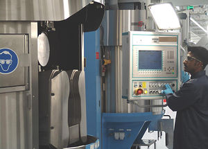
 [ download press photo ] | title: A hyperpure silicon ingot is sawn image text: A hyperpure silicon ingot is sawn into wafers. The wafers undergo further processing before delivery to customers. copyright: Siltronic AG |


