Contact:
Ariane Heim
Phone: +49 6196 - 66 3514
E-Mail: ariane.heim@samsung.de
| Pressbox |
 |
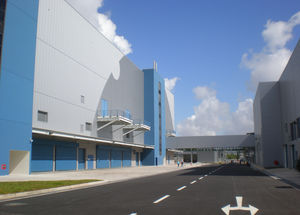
| The new silicon wafer plant of Siltronic |
| [ photos ] |
Singapore (pts006/19.06.2008/07:00) - * Plant officially commissioned after only 18 months of construction
* Target capacity of 300,000 wafers a month
* A US$1 billion investment
Siltronic Samsung Wafer Pte. Ltd., a joint venture of Samsung Electronics Co. Ltd. and Siltronic AG, today commissioned a new fab in Singapore for the production of 300 mm wafers. The facility officially started operation in an opening ceremony attended by Singapore's Prime Minister Lee Hsien Loong. After only 18 months of construction, Samsung Electronics, a leader in advanced semiconductor technology, and Siltronic, a subsidiary of Germany's chemical group Wacker Chemie AG, now own one of the world's largest and most advanced factories for 300 mm wafers. By 2010, the joint venture should reach a monthly capacity of 300,000 wafers and provide over 800 jobs. The overall investment in this project amounts to US$1 billion.
In his speech, Siltronic CEO and Wacker Chemie AG Executive Board member Wilhelm Sittenthaler emphasized the joint venture's strategic importance: "Today's commissioning is a key milestone in further expanding our presence on Asia's growth markets. Siltronic Samsung Wafer's ability to complete this new plant on schedule and in record time underscores the joint venture's engineering expertise and the outstanding collaborative strength between Samsung Electronics and Siltronic."
Oh-Hyun Kwon, president of Samsung Electronics' Semiconductor Business division, expressed particular appreciation with the punctual start of production in Singapore: "The new 300 mm wafer fabrication plant is a result of the strong local support from Singapore's Economic Development Board and the technology expertise of our partner, Siltronic. Together with Siltronic, Samsung anticipates Siltronic Samsung Wafer to play a significant role as a steady source of quality 300mm wafers at a time of rapid growth in the 300 mm wafer market segment."
"I congratulate the management and staff of Siltronic and Samsung who have worked together to bring this joint venture about, and to implement this project so expeditiously. This plant is a key addition to our vibrant semiconductor ecosystem", said Singapore's Prime Minister Mr. Lee Hsien Loong. "It will extend Singapore's semiconductor value chain, and bring us to the next level of wafering technology. The long-term prospect for the semiconductor industry remains bright and Singapore has positioned itself to take full advantage of this and remain a leading manufacturing location in Asia for electronics and semiconductors."
Company Profile - Samsung Electronics
Samsung Electronics Co., Ltd. is a global leader in semiconductor, telecommunication, digital media and digital convergence technologies with 2007 consolidated sales of US$103.4 billion. Employing approximately 150,000 people in 134 offices in 62 countries, the company consists of four main business units: Digital Media Business, LCD Business, Semiconductor Business, and Telecommunication Business. Recognized as one of the fastest growing global brands, Samsung Electronics is a leading producer of digital TVs, memory chips, mobile phones and TFT-LCDs. For more information, please visit www.samsung.com.
Company Profile - Siltronic
Siltronic AG - a subsidiary of Wacker Chemie AG - is a global leader in the market for hyperpure silicon wafers and a partner to many top-tier chip manufacturers. Our production facilities in Europe, the USA, Asia and Japan develop and manufacture wafers with diameters of up to 300 mm. Silicon wafers form the basis of modern micro and nanoelectronics. They are used, for instance, in computers, cellphones, the internet, DVD players, flat-panel displays, navigation systems, airbags, computer tomography equipment, aircraft control systems and many other applications. To find out more, visit www.siltronic.com.
Company Profile - Siltronic Samsung Wafer
Siltronic Samsung Wafer Pte. Ltd. is a joint venture between two global giants in their respective fields Siltronic and Samsung. Siltronic Samsung Wafer operates the first 300 mm wafer production fab in Singapore and also houses Singapore's first 300 mm crystal growing facility. Its new production complex is located in Tampines Industrial Park in Singapore, built with an investment of US$1 billion and the support of the Economic Development Board of Singapore. This makes the joint venture one of the top five investments in Singapore in 2006. By 2010, Siltronic Samsung Wafer expects to reach a monthly capacity of 300,000 wafers and to provide over 800 jobs.
For further information, please contact:
Wacker Chemie AG
Christof Bachmair
+49 89 6279 1830
christof.bachmair@wacker.com
Samsung Electronics Co., Ltd
Sunghae Park
+82 31 209 7037
sunghae_park@samsung.com
for region EMEA:
Ariane Heim
+49 6196 66 3514
ariane.heim@samsung.de
Siltronic AG
Kai Knitter
+49 89 8564 3210
kai.knitter@siltronic.com
This press release contains forward-looking statements based on assumptions and estimates of the executive boards of WACKER, Siltronic and Samsung Electronics. Although we assume the expectations in these forward-looking statements are realistic, we cannot guarantee they will prove to be correct. The assumptions may harbor risks and uncertainties that may cause the actual figures to differ considerably from the forward-looking statements. Factors that may cause such discrepancies include, among other things, changes in the economic and business environment, variations in exchange and interest rates, the introduction of competing products, lack of acceptance for new products or services, and changes in corporate strategy. WACKER, Siltronic and Samsung do not plan to update the forward-looking statements, nor do they assume the obligation to do so.
(end)
|
 |


